
Transistor:
- Basic building blocks in all of the electronics.
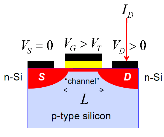
- MOSFET Cross Sectional view:

- MOSFET Top view:

- Metal Oxide Semiconductor Field Effect Transistor.
- Fabricated on a p-type Silicon.
- n-channel transistor (shown above):
- Source (S) of charge carriers.
- Drain (D).
- Silicon Dioxide (SiO2) thin Gate in between:
- Applying enough voltage will turn-on the transistor.
- Top view, in the above figure, shows source and the drain on left and right, respectively.
- Gate in the middle.
- Current is proportional to the width - more width (W) = more current.
- Initial transistors were discrete, packaged up inside a package with a few leads, and electronic circuits were made using these (shown below).
- Initial Integrated Circuits were put into a single slab of silicon called a silicon chip, and wired. First chip example - Intel's 4004 microprocessor with 2300 transistors wired together (shown below).
 |
| 4004 Image Courtesy - Intel. |
- Considering the transistor as a black box with silicon inside it containing the transistor design, it has three leads coming out (see below) and a fourth lead sometimes.

- In the above diagram, a large amount of current flows through terminal 1, and terminal 2. There is another Terminal which controls current through t1 and t2.
- Types of transistors:
- SOI MOSFET, FinFET, SB FET, MODFET (HEMT), TFT, bipolar transistor, JFET, heterojunction bipolar transistor, BTBT FET, SpinFET, etc.
- Actual MOSFET:
 |
| Image Courtesy - Texas Instruments. |
- Circuit symbol (terminal 4 is body in this case):

- Modern MOSFETs - FinFET: most modern technologies now use this type.

- In FinFETs, a thin fin of silicon sticks upwards vertically and the Gate wraps around.
- Operating principle is similar to MOSFET.
- In MOSFET, let us study some I - V characteristics of a n-MOS: Id(Vg, Vs, Vd)


- Two input leads, and two output leads: In this case, it is a common source configuration. Here, source is one of the input terminals as well as an output terminals (see above diagram).
- Transfer characteristics: Output current as a function of voltage between gate and the source, Id (Vgs) at a fixed Vds - output voltage between the drain and the source.
- Output characteristics: Output current as a function of the output voltage, Id (Vds) at a fixed Vgs at a fixed value.
- Starting with a simple example, the I - V characteristics of a Resistor:


- Ohm's law: current is voltage divided by resistance (I = V/R), let us not get into physics and derive this using Maxwell's equations.
- IV characteristics is a plot between current and voltage, when the current through a resistor is a function of the voltage between the two terminals, a straight line.
- More resistance means less current, and less resistance means more current (as shown in the above plot).
- Ideal current source IV characteristic:


- IV characteristics of a MOSFET (using n-channel MOS transistor):


- Apply small voltage between drain and source called Vds, the IV characteristic looks like a resistor - where device operates as a gate voltage controlled resistor. On applying large enough voltage between d and s, the IV characteristics acts like an ideal current source - independent and saturated of the applied voltage.
- On changing gate voltage applied in small amount, we can change the slope - like a resistor.
- Non-Ideal characteristics of a current source: Ideal current source in parallel with a resistor.


- Non-Ideal IV characteristics of a n-MOS transistor:


- MOSFET IV output characteristics: output current Id, vs the output voltage Vds

- Each plotted line shown above is at a different input voltage, Vgs.
- The rising part of the plot is called the linear region, and the horizontal slope part of the line is called the saturation region. If voltage is less than Vdsat, we are in the linear region as shown in the above plot.
- Subthreshold region - this is close to zero current Id, when the device doesn't turn on thus no current flows. The gate voltage Vg has to be big enough to turn on the device so that we can see the current starts flowing beyond that voltage.
- Output vs Transfer characteristics of a transistor:


- Applying a low voltage on the Drain and Source, and then analyzing it in reference to higher voltage between the drain and the source.
- High voltage between D and S means higher current Id.
- No current flows until the voltage is big enough, and then the current shoots up. This voltage is called the threshold voltage of the transistor (Vt).
- Applications of MOSFETs:
 |
| Symbol |

- Can be used as a digital switch - on or off.
- It can be used as an analog device - amplification of a signal.
- Types of MOSFETs:
- N-MOSFET - side view
- N-channel transistor: charge carriers are negatively charged electrons flowing from the source to the drain, thus current flows-in from the drain.
- Vg is applied gate voltage which should be more than the threshold Vt.
- modern day - CMOS technology.
- P-MOSFET -side view
- It is complementary to NMOS.
- It has positive charge carriers flowing from S to D. Current flows out of D terminal.
- To connect the channel from S to D, the gate voltage Vg should be less than threshold voltage, Vt.
- Vt is a negative value, and Vg is even more negative value.
- Mainstream / modern-day technology is the CMOS technology.

- There is always a n-channel device paired with a p-channel device.
- Transistors are three or sometimes a four terminal devices that can control a large output current with an input voltage or sometimes with a small input current.
- Transistors can act like a voltage controlled resistor or a voltage controlled current sources when we apply a large voltage between the drain and the source.
- The IV plot shape makes transistors useful for both digital and analog circuits. IV plot is determined by the physics behind it.
Device Metrics:
- nMOS and pMOS:
- In n-MOS, the electrons carry the current through n-channel, when the switch is closed the current flows and critical voltage is less than threshold voltage.
- In p-MOS, indicated with an open circle on the gate. The current is carried by holes / positive charge carriers. In order to close the switch and allow the current to flow, Vgs is less than (more negative) than the threshold voltage.


- CMOS Inverter: Using both nMOS and cMOS building blocks, we create a device called CMOS inverter. The n-MOS is at the bottom, and p-MOS at the top. The nMOS is grounded and the gates of both nMOS and pMOS are connected together, and the drain of both are connected to the output 'Vout'. The p-channel transistor is upside-down. The pMOS source 'S' is connected to the most positive voltage of the circuit Vdd.

This comment has been removed by the author.
ReplyDeleteLianli.Tech specializes in cryptomining cooling solutions, offering cutting-edge technology to optimize mining performance and efficiency. Their innovative cooling systems help miners maintain stable temperatures, reduce energy consumption, and extend hardware lifespan. With a strong focus on advanced thermal management, Lianli.Tech provides high-quality, reliable solutions tailored for both small and large-scale mining operations. Whether you're dealing with air, liquid, or immersion cooling, their expertise ensures maximum profitability and sustainability in crypto mining. Explore their solutions to enhance your mining setup today to know more visit at:- https://lianli.tech/
ReplyDeleteHashZebra.io is a trusted provider of cryptocurrency mining solutions, specializing in Antminer hardware for maximum efficiency and profitability. Whether you’re a beginner or an expert miner, we offer top-tier mining equipment, hosting services, and expert support to optimize your operations. Our advanced cooling solutions and power management ensure that your Antminer runs at peak performance. At HashZebra, we are dedicated to making crypto mining seamless, reliable, and profitable with the latest technology and industry-leading solutions. to know more visit at:- https://hashzebra.io/
ReplyDelete