
This post is Sponsored by: Track Your Conceptual Progress on Electronic Design into a journal perfectly designed by Phoenix Skyewalker (buy on amazon).
What is an FPGA?
- FPGAs (Field Programmable Gate Arrays) are highly flexible integrated circuits, offering the ability to be reprogrammed after deployment. This makes them ideal for adapting to new requirements, fixing issues, or upgrading features without replacing hardware, which is especially useful in remote settings.
- FPGAs consist of configurable logic blocks (CLBs) and programmable interconnects that allow designers to create anything from basic logic functions to more complex operations (Arm Ltd., n.d.). They also support parallel processing, enabling multiple tasks to be executed simultaneously in hardware, unlike CPUs that process instructions sequentially. This leads to lower latency and faster performance for specific workloads.

Types of FPGAs:
- SRAM based FPGAs: These FPGAs use Static RAM (SRAM) to store configuration data, which makes them reprogrammable as many times as needed.
- Highly flexible and reconfigurable.
- Configuration data is volatile and needs to be reloaded after power-off.
- External memory or a configuration ROM is required to reload the FPGA.
- Example: Intel Altera Max 10 is an SRAM based FPGA that uses an Internal Flash Memory that holds the configuration. During power down all contents of SRAM is lost, hence during POR the internal flash quickly reloads the configuration.
- Hybrid FPGAs (SoC FPGAs):These combine an FPGA with a hard processor core (usually an ARM CPU) on the same chip, creating a hybrid system-on-chip (SoC).
- Offers both software flexibility (with the processor) and hardware acceleration (with the FPGA).
- Ideal for complex systems that need both general-purpose computing and custom logic in one package.
- Xilinx Zynq and Intel Altera Agilex Family.
NOTE: Based on the FPGA you choose, the HW design steps would change. That being said overall the fundamentals stay the same.
Choosing an FPGA:
- FPGA Engineers usually look at the Logic cells, IPs available to port/fit a design. Also software requirements dictate if you need a SoC FPGA vs Traditional SRAM based FPGA. In our example we are selecting an SoC FPGA by Xilinx: XC7Z010-2CLG400I
Feature Overview:
- Dual ARM® Cortex®-A9 MPCore™ with CoreSight™ System On Chip (SOC)
- Logic Cells: 28K
- Processor
Power:
Unlike traditional SoCs, FPGAs power requirements based on Toggle rate of IO blocks and use of number of IO Blocks. FPGA vendors provide Power Thermal Calculators in order to make early estimates in order to size the DC-DC Converters per rail.
In our example:
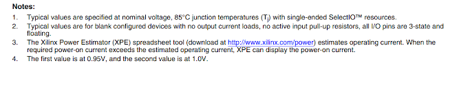
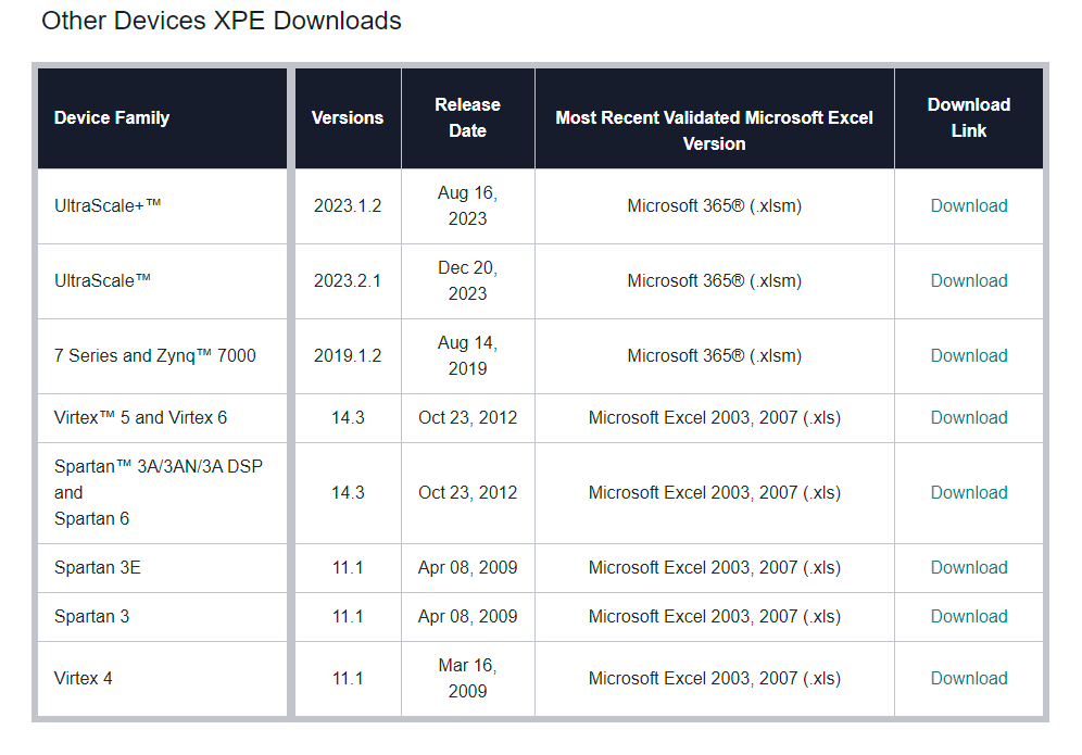
Xilinx provides a spreadsheet tool inorder to estimate these rails. You do need to signup in order to Download this tool.
FPGAs are very particular about noise tolerance and di/dt response to these voltage rails. Designers need to evaluate and do a detailed PDN analysis in order to validate their DC-DC solutions.
- Post Contributor & Author: Nilanjan Talukder (SemiSaga)
Comments
Post a Comment